Designing with Eagle
Schematics
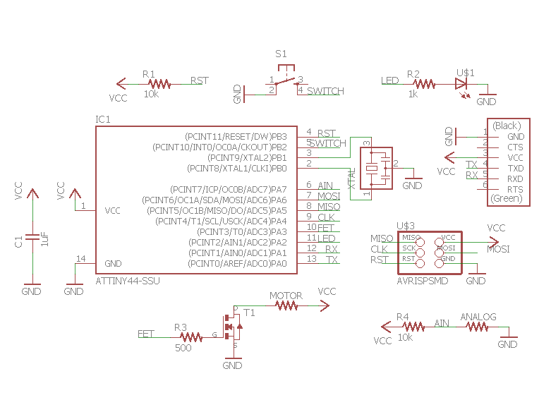
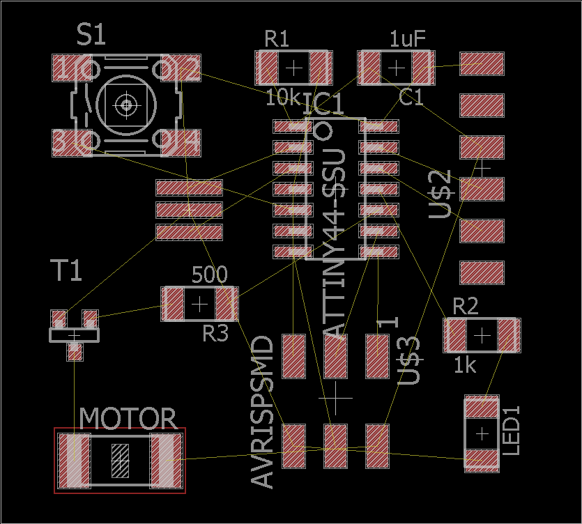
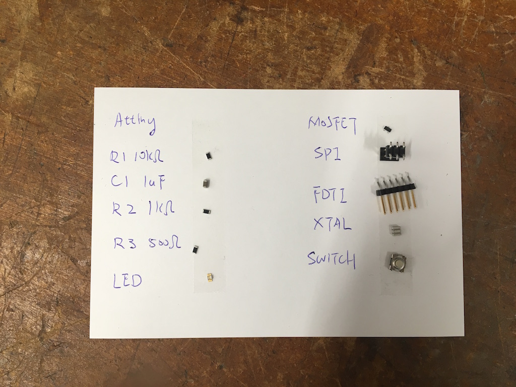
I used eagle to design a board similar to the Echo helloworld board, which can echo messgae computer send to it. And I added a LED, a switch and a MOSFET which I intend to use to drive a motor and test the PWM function of the microcontroller. The first step in electronic design is draw the schematics.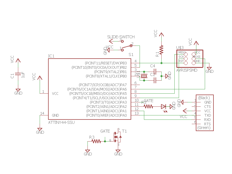
Routing
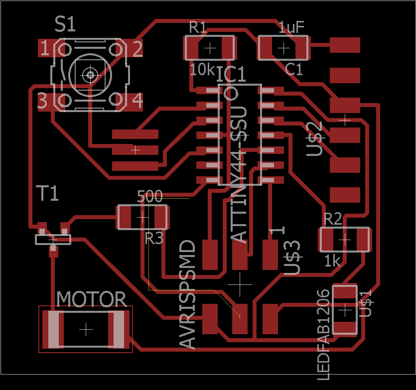
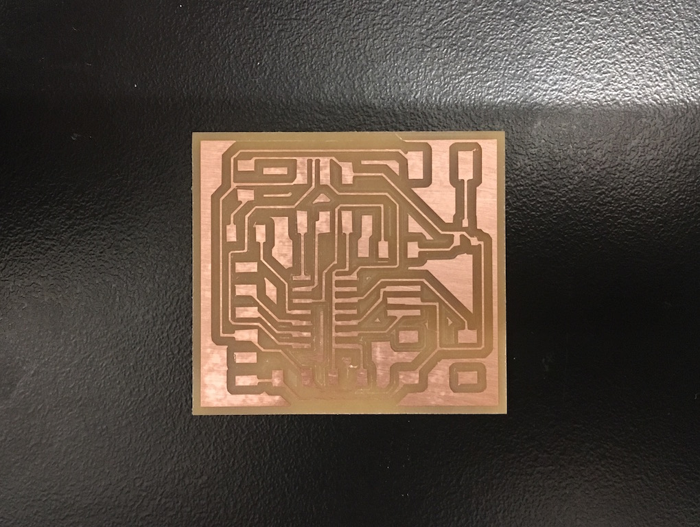
Next step is routing the connections by going to board enviroment in eagle. First move around the component to desired position and to unravel as many connections as possible. While doing that, keep clicking ratsnest to clean up the connections. Then I setup the design rules in the net class, and set the minimum seperation to 15mil which is our 1/64' bit size. I used auto-routing first and found there are few connections that cannot be made be auto-routing. And after analysing the connectiong, I decided to remove the analog input and moved a few component around. Then the auto-routing is able to find the right connection for me as shown. I also ripped off a few wires and reconnected them myself to get exactly I want.
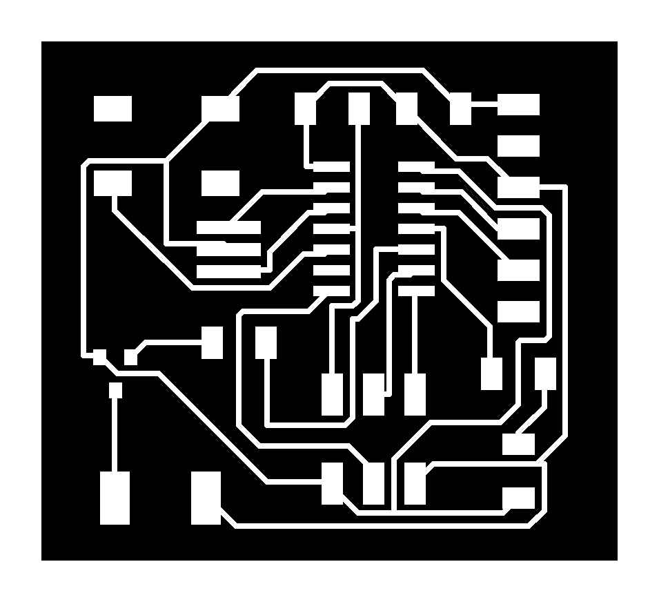
 I export the end result in png with 600ppi and in photoshop I enlarged the canvas by 0.1' and exported the route file. Then I inverted the color and filled the middle with white and generated the outline cut.

Production
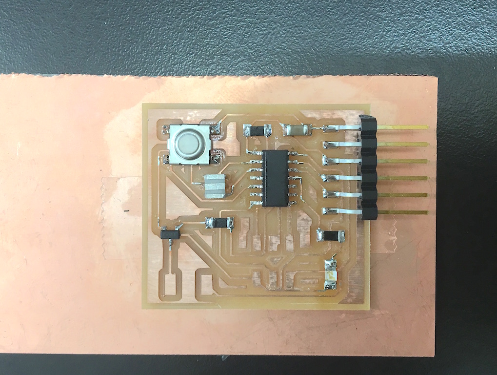
I cutted the board and it looked fine at first glance. So filled the board, and when I am half way into it, I fount there are few places not milling into as the gap is small. ALthough in the design rule, I set the minimal gap to be 15mil, the rowlang milling machine won't get into it. Because it's half way done, I tried to scatch off the tiny connection with a knife and it worked.
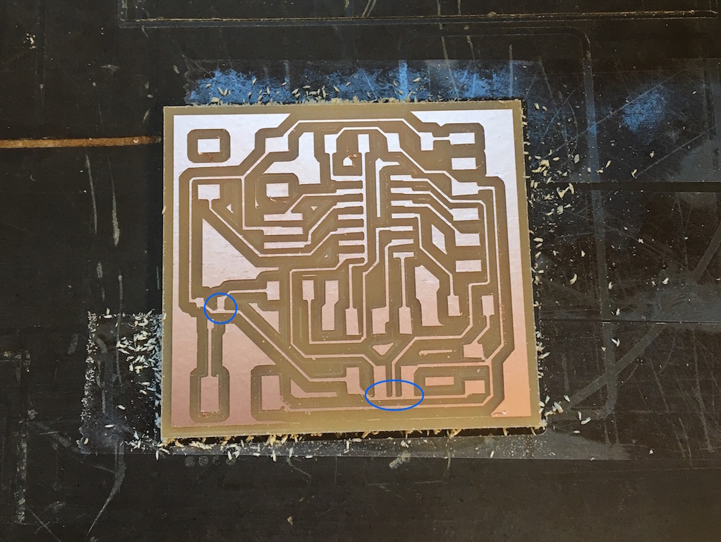
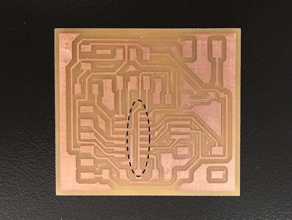
While I keep populating the board, I found there was two more un-milled seperations. I scatched the same way and test if it's insulating using multi-meter. However, it didn't notice the previous user set the test mode in diode and after I switch back to resistance mode, I found many connections are short to each other, and it turns out my micro-controller is fried. Then I attempt to de-solder the micro-controllerm which turns out to be really hard. I start with the braid to remove most of the solder, then I use a tweezer to drag each pin up while heating it with solder gun. In the end I manage to remove the microcontroller but break off one of the copper pad as shown below.
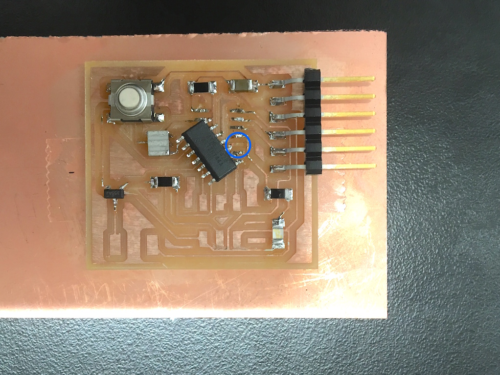
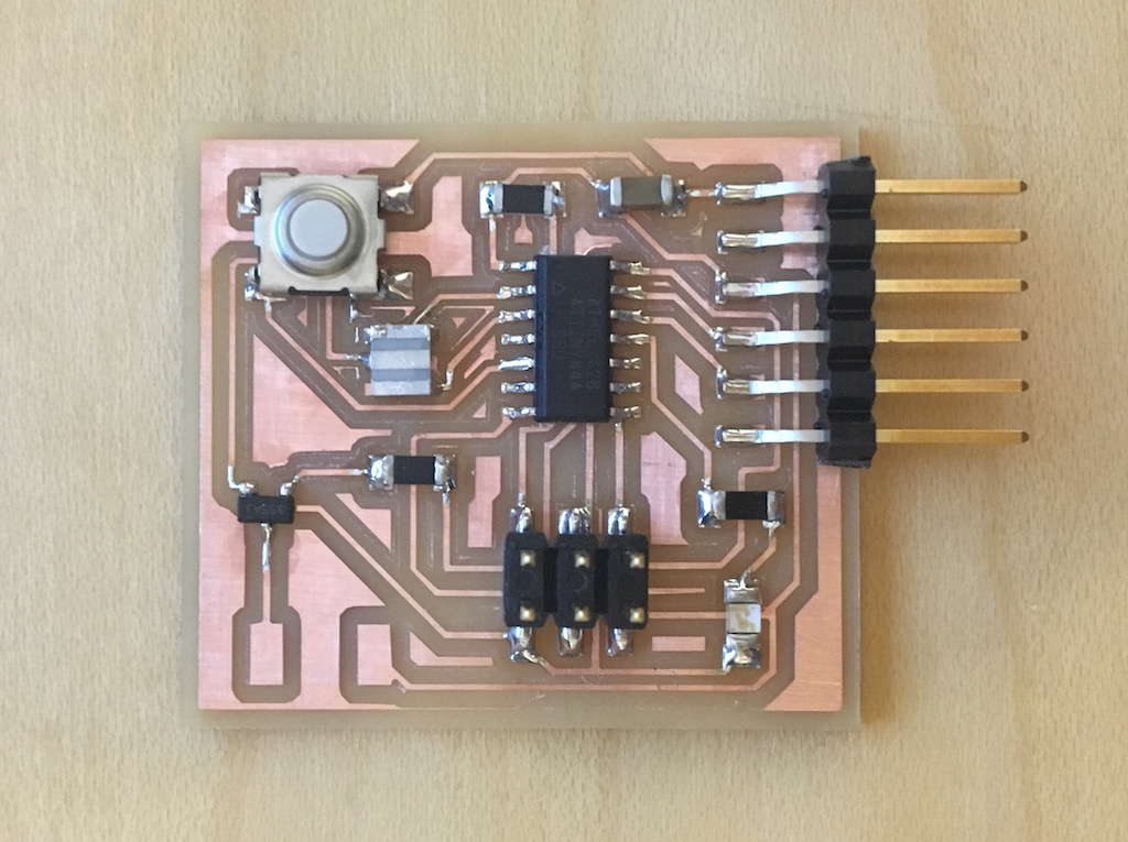
So I have to make another board. And I enlarged the gaps which didn't mill through last time in image editing software. (Update) When stuffing the board, I found the reason of the pins shorted together is actually not a broken ATtiny 44, instead all the connections are shorted due to non-through cut as shown below. I used a knife to open the connections are finished the task. Later in the design, I need to pay special attention to small clearence cut to avoid the situation.